

Key Insights: LED die characteristics including available wavelengths, selection criteria, and operational considerations.
Light emitting diodes (LEDs) have advanced significantly over six decades and are no longer just tiny display lights used solely as indicators. They have found a significant niche in low-cost, long-lifetime, high-power illuminators for numerous applications in medical, multispectral, industrial, solar, and semiconductor markets. As environmentally friendly light sources, LEDs often serve as superior alternatives to arc lamps and lasers when operated at their full potential. The evolution of LED light sources raises key questions about available options and the selection process.
What is an LED?
LED stands for Light Emitting Diode which is fundamentally a semiconductor that converts electricity into photons when current flows through it. The wavelength of the emitted light is a function of the energy band gap of the semiconductor materials used (e.g. AlGaN, InGaN, AlGaInP, AlGaAs, InGaAsP) and ranges from UVC to NIR. Materials with larger energy bandgaps emit shorter wavelengths and materials with smaller energy bandgaps emit longer wavelengths. Bare LED die are Lambertian emitters, and, as such, the light is equally bright in all directions, regardless of the viewing angle. The surface-emitting diode structure is used most often (as opposed to edge-emitting) because it produces light over a broader angle. Clever optical systems must be designed to maximize photon collection, while considering etendue. Unlike lasers, LED light is incoherent, and does not cause speckle, which decreases uniformity. LED spectral bandwidth is broader, which is often better for photoinitiators used in 3D printing, UV curing, and medical applications, though the output can be filtered for a narrower spectral range.
LED die size and structure vary, but for Innovations in Optics, Inc. (IOI) applications, the die active area for surface emitters is usually between 0.9 and 1.2 mm square. To optimize light collection and output, multiple LED die can be close-packed in chip-on-board (COB) arrays, which enable the creation of multi-wavelength illuminators that offer significant flexibility and ease of tunability. LEDs switch on and off extremely fast – on the order of nanoseconds – making pulsed operation at higher currents feasible with appropriate cooling and duty cycles. LEDs are among the longest-lived illuminators with lifetimes that can exceed 100,000 hours depending upon the mode of operation.
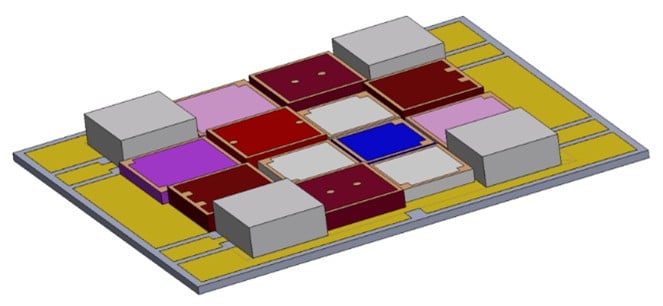
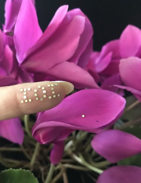
Figure 1: 4×4 array of close-packed LED die shows variation in size and height for deep UV through NIR LEDs that requires special consideration for die attach, wire bonding, and cooling.
LED Characteristics and Selection
Manufacturers produce LED die for wavelengths ranging from lower UV to NIR, but output power and efficiency vary. Consequently, manufacturers sort and sell them in groups, called bins, according to power and wavelength ranges. Multiple bins of LED die exist in the UVA, visible, white, and NIR wavelengths. Figure 2 illustrates a sampling of die used at IOI, though not all bins are shown. Deep UV die below 365nm are flip-chip type.
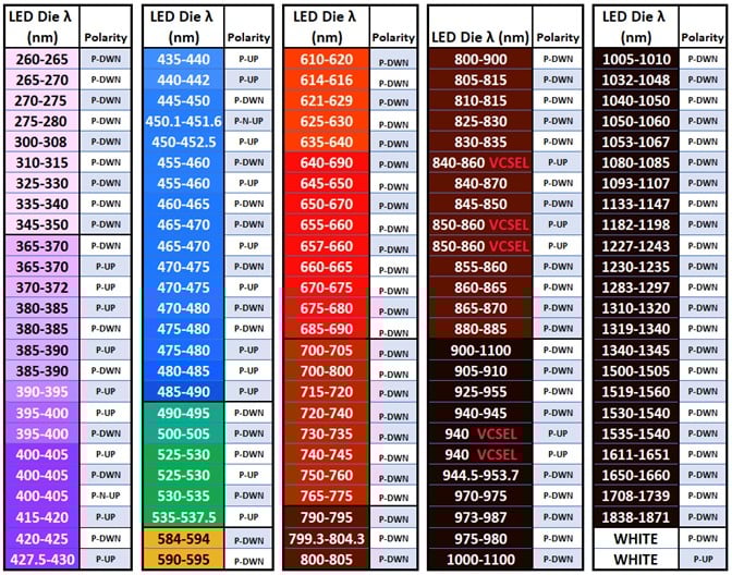
Figure 2: LED die options UV – VIS – NIR include die of different polarity, size, structure, spectral bandwidth, and binning range. Not all die are shown.
For UV die, readily available wavelengths are often binned as narrowly as 5nm, whereas for NIR die, bins are broader – on the order of 100 nm for wavelengths nearing 2400 nm. Bare LED die also vary in configuration. Deep UV LEDs (e.g. 260 nm, 265 nm, 275 nm, 280 nm, 308 nm, 315 nm, 325 nm, 340 nm) utilize a ‘flip-chip’ design with AlGaN. These are favored for applications such as disinfection and fluorescence spectroscopy, though they produce an order of magnitude less output than the traditional chip designs used for UV wavelengths above 365 nm. Thus, flip-chip LEDs require a special board design to accommodate the surface mount technology (SMT) configuration of electrical contacts on the bottom, as well as specialized thermal management to maximize output. Most LED die emitting at 365 nm and above have contacts on the top, allowing wire bonding to connect the anode and cathode. Figure 3 shows both the flip-chip and regular chip configurations.
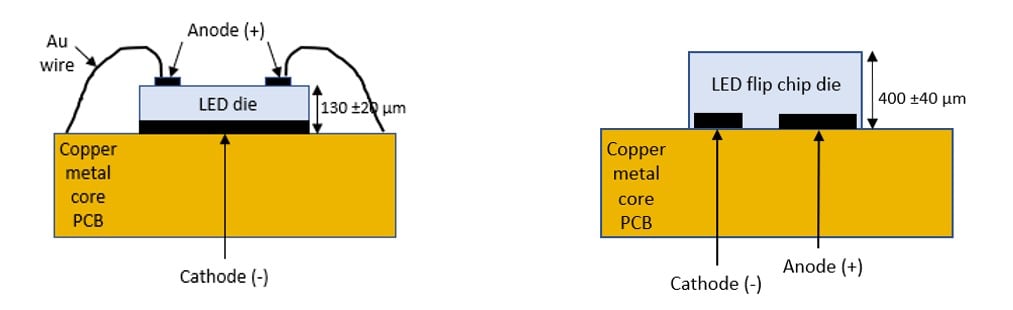
Figure 3: Regular LED chips ( > 365nm) require wire bonds, but LED Flip-chip (deep UV) has electrical contacts placed on the bottom and attaches directly to the PCB or heat sink.
The spectral shape of an LED die is influenced by drive current, die junction temperature, and wavelength. As drive current or die junction temperature increases, peak wavelength shifts – shorter for UV die and longer for IR die. The full width at half-maximum (FWHM) is broader for longer wavelengths and increases further as temperature increases. Consequently, specifications for a given application must be well-defined and considered in this context. Figures 4 and 5 show spectral behavior examples for UV and NIR. Longer-wavelength LED die tend to experience greater loss and spectral shift with changes in junction temperature.
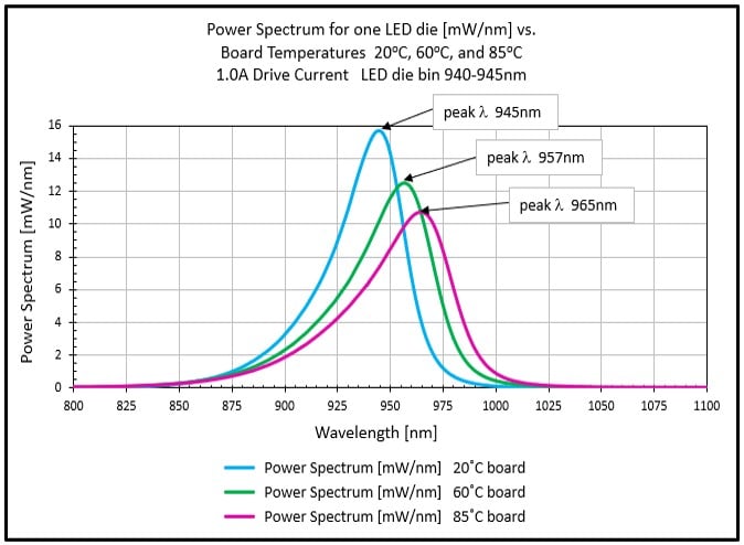
Figure 4: Peak wavelength shifts longer, FWHM broadens, and optical power decreases with an increase in board temperature for this 940nm LED die.
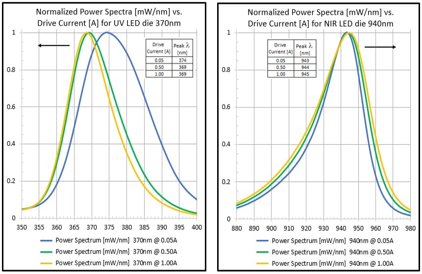
Figure 5: Higher drive currents cause a shift to shorter peak wavelength for the UV and a shift to longer peak wavelength for NIR.
For copy exact applications, it is also important to track the parameters on a given die sheet, which may differ from sheet to sheet while still remaining within the specified bin. Stability and uniformity of the spectral output are critical in obtaining high accuracy. Thus, understanding die characteristics and behavior provides insight into appropriate thermal management.
Over a broad range of wavelengths (UV-VIS-NIR), LED die have different polarity, a feature of the die that has implications for the electronics’ design. Mixing die of different polarities requires more complex drivers. Several terms describe polarity as shown in Figure 6. P-up is also known as common cathode or cathode-down, meaning the cathode is ground and the top is positive relative to the LED bottom. This is typical for UV through green and white LED chips. P-down, known as common anode or cathode-up, has the anode at ground attached to the LED board with wires bonded to pads on top. LED die with wavelengths from amber (590 nm) through NIR are typically P-down. IOI designs and manufactures both single-polarity and mixed-polarity light engines.
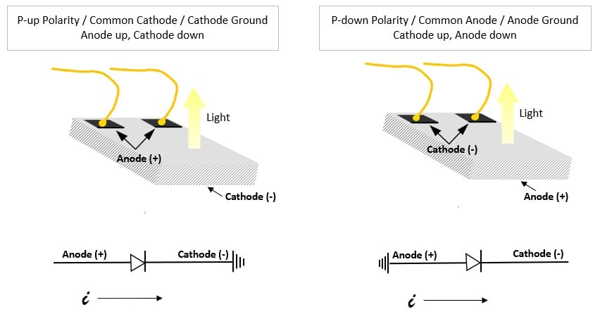
Figure 6: One LED die each with P-up or P-down polarity and associated terminology.
Operating Tips
Most off-the-shelf LED die have current ratings in the milliamp range. High-power LEDs, such as those used for IOI illuminators, can be driven up to 3A per die or more, producing several watts of light per LED die. However, operating at high driver currents requires extensive knowledge, techniques, and intellectual property (IP) to manage thermal loads and keep die junction temperatures low. Otherwise, the die can fail in seconds. For example, IOI LED boards incorporate a built-in thermistor for temperature monitoring and offer multiple options for air or liquid cooling. As a rule of thumb, for every 10˚C lower junction temperature, lifetime increases by a factor of two. Additionally, as die junction temperature rises, quantum efficiency decreases. The goal is to achieve high output while ensuring tens of thousands of hours of LED lifetime.
LEDs are current-sensitive devices, and, like other diodes, their current depends exponentially on voltage. A small voltage change can cause a large current variation, making operation with a voltage source ill-advised. Each LED die has a specific polarity, and an associated forward voltage determined largely by the bandgap energy of the material. These characteristics impact LED driving methods. Precise current regulation is essential and typically achieved with a constant-current power supply that provides protection against over-current, over-voltage, and over-temperature conditions. Users must ensure proper current flow direction and stability.
If all LED die are tied to the same substrate at the bottom, a ground-based current source is required for P-up polarity (anode on top), whereas for P-down polarity (anode on bottom) a current sink is needed. If a non-ground-based driver is used for P-down (common anode) die, the LED board must be electrically isolated (e.g. with a non-conductive thermal pad). Current flows through an LED only from the p-doped region to the n-doped region, and a reverse voltage of only a few volts can destroy the LED.
Conclusion
With LEDs available in a broad range of wavelengths and at ever-increasing power levels, numerous markets benefit from their use. Achieving the most successful state-of-the-art solutions for high-power illuminators requires knowledge and experience in LED characteristics and performance across a wide range of conditions. Thus, understanding LED selection and the nuances of operating LEDs within a system is crucial.
Rapid improvements in high-power LED technology have enabled efficient, long-lifetime illuminators that are quickly replacing arc lamps and lasers in applications such as multispectral and hyperspectral imaging, fluorescence, lithography, endoscopy, solar simulation, materials testing, 3D printing, inspection, sorting, machine vision, and PCB manufacturing.
LEDs are radiant with potential.